Ion Beams
 WBGM Project
Wide Band Gap Materials: the group have been involved in research projects to investigate the damage
has build-up processes during
ion irradiation and to test their performance as radiation detectors and LED's.
WBGM Project
Wide Band Gap Materials: the group have been involved in research projects to investigate the damage
has build-up processes during
ion irradiation and to test their performance as radiation detectors and LED's.
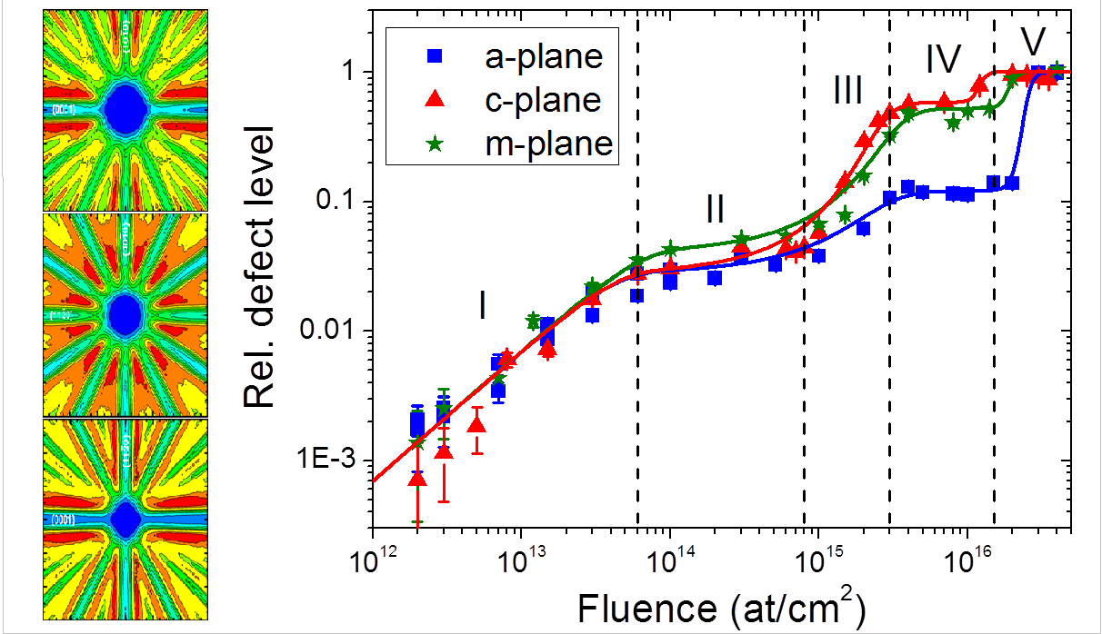
Implantation damage build-up curves measured along these crystal directions revealing strong radiation resistance
and channelling patterns along the a, c and m axes in GaN.
 MEC Project
Materials for Energy Conversion: high solar absorption can be achieved using coating with a graded refractive index and extinction
coefficient and the study of these systems are at the core of the project.
MEC Project
Materials for Energy Conversion: high solar absorption can be achieved using coating with a graded refractive index and extinction
coefficient and the study of these systems are at the core of the project.
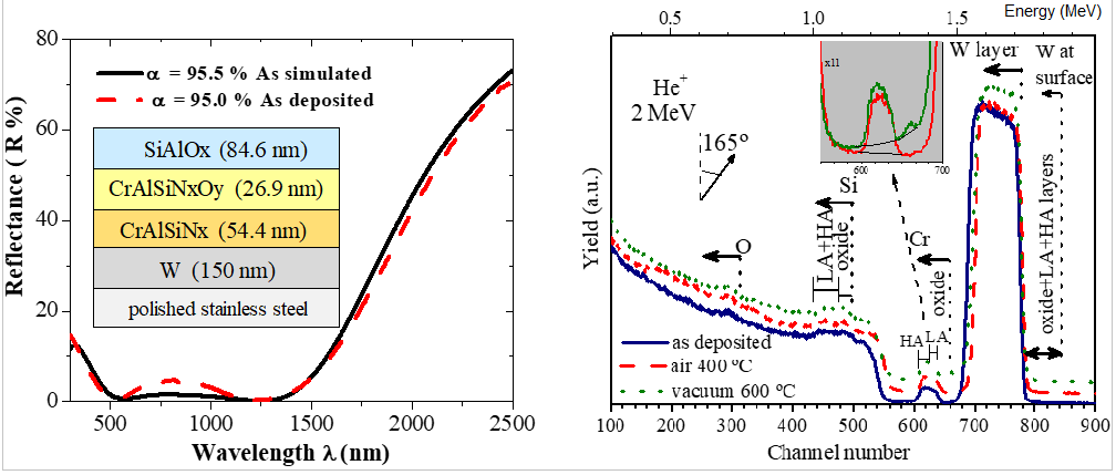
Simulated
and experimental reflectance curves of the absorber in the
figure as well as the RBS spectra of the as deposited stack, after air annealing at 400 °C and vacuum annealing at 600 °C, both for 650 h.
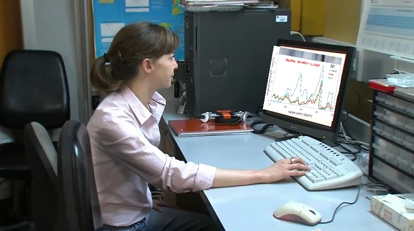 JET2 Project
Joint European Torus 2: study of the physics underlying all the processes related with
the plasma wall interactions. The group is responsible for the analysis of marker tiles and passive diagnostics components
from the main chamber and divertor of JET.
JET2 Project
Joint European Torus 2: study of the physics underlying all the processes related with
the plasma wall interactions. The group is responsible for the analysis of marker tiles and passive diagnostics components
from the main chamber and divertor of JET.
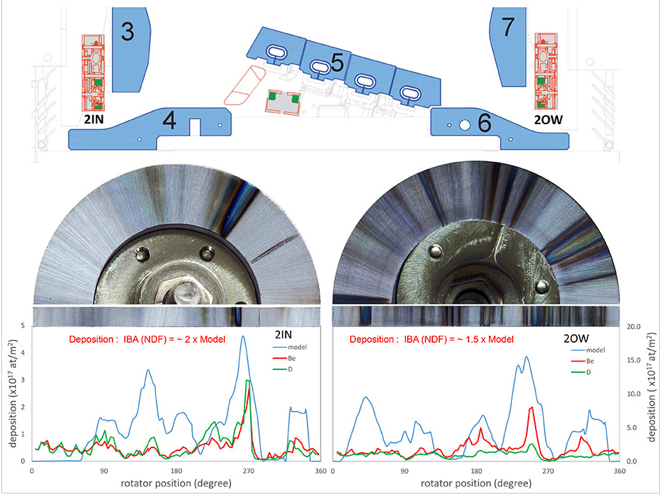
Beryllium and Deuterium deposition on the inner (2IN) and outer (2OW) collectors for ILW 2 campaign.
The red line represents the model for the Be deposition.